Posted on Leave a comment

DMA Autobuffering techniques

For high speed DMA throughput where you’d want the least interruptions, several CPU cores on the higher end deploy scatter-gather style DMA engines to avoid slow memory copying. Let me give an example:

  1. Assume you would want to compose a network package and stream it out to a media access controller IP core (MAC)
  2. You have one Ethernet/IP/UDP/RTP header or alike and you are not planning to change it much during a streaming session
  3. Your payload might be in memory, but also coming from an external data port (such as a video data)
DMA descriptor scheme

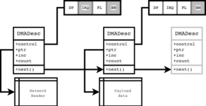
The DMAA core (part of the cCAP families starting with ‘d’, like dombert) allows to set up descriptors in a special shared (and fast) dual port memory such that the DMAA engine can stream almost continuously to a peripheral. Likewise, descriptors can be set up for input streams (peripheral to memory), if required. The above image should talk. You start the DMA engine by writing the descriptor address into the DMAA_START_DESC register. Once the transaction has completed, an IRQ will be fired (which will for example allow you to update the sequence number of an RTP packet). Meanwhile, the DMAA engine will fetch the NEXT descriptor pointer (next()) and stream the payload data pointed to by ptr. You just have to make sure the IRQ routine does not waste too much time doing other things, if you use the same header in the following packet.

Note the control bits: an IRQ will for example only be fired, when the according IRQ bit is set. The EN bit tells the DMA engine to keep going after the current descriptor. The entire transaction stops when the last descriptor has the EN bit set to 0.

In the example for a MAC controller, you might want to append several chunks of data before actually issuing an Ethernet packet. How would the MAC know how long the packet actually is, without explicit (and timing critical) writing of length registers? This is taken care of by the FL (FLUSH) bit. Once a DMA transaction has completed and the FL bit is set, the packet is flushed in one go to the MAC and sent out immediately. The DMA engine waits until the data has been transmitted to the Packet FIFO and then resumes with the next descriptor.

In fact, this concept requires very little logic overhead and can run at high speeds even on small FPGAs (with a reasonable amount of memory buffers shared between DMAA and CPU core)

High speed streaming

When streaming high speed raw data, you might not want the CPU composing packets from external sources. Better stream them directly from the peripheral to the MAC the interleaved way. For the above Payload packet descriptor, the alternative data input method would be by setting the DP (DATAPORT) bit. In this case, the ptr and inc attribute of the descriptor are ignored and `count` number of bytes plus one are taken from the dataport input FIFO. If there is a premature end to the data, a CANCEL action can occur. The DMA will then stop (ignore the EN bit) and the user space program can react accordingly by checking if the DMAA engine is active. The effectively written number of bytes can be read from a DMA_CURCOUNT register and if necessary, padding action can occur.

Complex DMAA setup

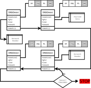
Likewise, receiving packets of a priori unknown sizes is possible using this approach. A receive DMA IRQ handler just checks this register and fills in the effective packet size in the receiver packet queue which is later polled by ‘user space’ (this being the bare metal main loop, typically).

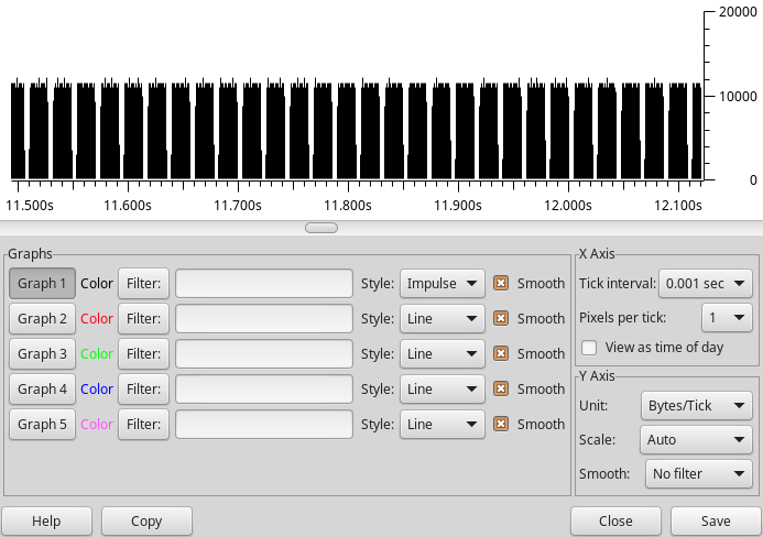
This way, data rates up to the theoretical maximum can be achieved. The rest is a matter of configuring the right packet and FIFO sizes. Below you can see a Wireshark packet graph for a regular packet burst (30 frames per second). As you can see, it’s cranked up to the maximum possible throughput during the burst.

Wireshark Packet burst

Summary

Advanced DMA capabilities are easy to implement in FPGA SoCs and make high speed transfers possible even with simple and slow CPUs.

Some reference applications:

  • Almost-Zero latency streaming of compressed Video over RTP (RealTimeProtocol)
  • Signal Analyzer and trace units (‘digital scopes’)
Posted on

ECP5 and SPI data overlay

As described in a previous blog post on playing with the ECP5 under Linux, I’ve ported a IoT and networking proven concept to the Versa ECP5G developer kit from Lattice. As we don’t want to use up the entire RAM for program code or data that is rarely used, another attempt was made on this platform to recreate the SPI cache trick implemented on Xilinx Spartan[3,6] hardware (Virtual ROM on small FPGAs).

The first blind run without reading the docs threw me an error: the SPI MCLK dedicated pin can not be used in “user mode”, i.e. after the FPGA has booted. Well, not as user pin, that is. However, the ECP5 has a specific primitive called USRMCLK which obviously allows to mux in a user defined clock to the MCLK pin. However, this requires you to turn off the MASTER_SPI_PORT option in the SYSCONFIG line of your preference *.lpf:

SYSCONFIG SLAVE_SPI_PORT=DISABLE CONFIG_MODE=JTAG CONFIG_SECURE=OFF TRANSFR=OFF MASTER_SPI_PORT=DISABLE SLAVE_PARALLEL_PORT=DISABLE MCCLK_FREQ=38.8 BACKGROUND_RECONFIG=OFF ;

The other SPI pins (MISO/MOSI/CS) again are accessed as normal user pins specified in the LPF. The SPI clock from the custom SPI IP core (there’s no hard IP as in the MachXO* platforms) is silently routed through the USRMCLK primitive to the MCLK pin after the boot process has finished. The USRMCLK also requires a tristate input signal (‘1’ = SPI clock not active). If you are tempted to use this as a clock enable: Don’t. Just feed the gated SPI clock to the usrmclki pin of the USRMCLK primitive and use the /CS signal of the SPI core for the usrmclkts pin.

The disadvantage of this solution: When MASTER_SPI_PORT is disabled, background programming of the SPI flash through the Diamond Programmer will no longer work. Every time you update, you will have to load another bit file with enabled MSPI before you can update the flash. Or alternatively, mess with the boot mode so that you have a default configuration allowing background programming.

On the other hand, we can now update the flash “in system” using a simple UART boot loader so we don’t have to wait for the somewhat painfully slow Programmer to finish.

Program layout

Using the linker script has already been described in (Virtual ROM on small FPGAs). Using this technique again, we relocate all seldom used programm code such as initialization code into the external program memory. We then end up with the boot ROM code in a pure HDL file (RAM initialization bit vectors) and a binary image containing the program/data overlay code. This image is created by a simple objcopy call from the Firmware Makefile:

zpu-elf-objcopy \
        -j .ext.text \
        -j .ext.rodata \
        -O binary main.elf flashdata.bin

This is assembled using the Deployment Tool of the Diamond Programmer, found in the Utilities menu. This tool creates an intel hex file (*.mcs) from the BIT file and an attached flashdata.bin that you can select under the “User Data Files” tap in the Advanced SPI flash creation wizard. Finally, this MCS file can be burned into the SPI flash using the boot loader command:

# bl                                                                            
> Waiting for data..

Then simply upload the mcs file to the target inside your terminal program. Then you can hit the PROG button (not the global reset) to load the new image. Note that there are no safety checks at this moment, an illegal image will not boot and you will have to use the Programmer again.

SPI flash filesystems

A nice way to store files (such as default settings) on the target is by using the OpenSource spiffs tools. It may not fit into the standard configuration though, the library itself is roughly 36k in size. You could try to put parts of it into “overlay”, but it is probably safer to keep it in L1 memory and increase that by another power of two.

This is the repo we use:

https://github.com/pellepl/spiffs.git


Posted on Leave a comment

Hacking your own FPGA chip scope

Ok, why would we want to do that, when there are various existing solutions:

  • Altera SignalTap
  • Xilinx ChipScope
  • Lattice Reveal

Make a long story short: To be in control! Well, there were some quirks with existing code, some tools wouldn’t run on my OS, and I wanted to be vendor independent.

But one major reason: We wanted to debug our own DSP core based system while eavesdropping on some internal signals.

So there we go with the shopping list:

  1. JTAG port and TAP implementation [already done]
  2. JTAG agent for debugging and BSCAN register monitoring [already done]
  3. Output to ‘live’ wave display

So again, a little hack of a VCD output got me going. Basically, a specific JTAG register is continously polled in the main loop and the output is written to a VCD file. Like we did it here (JTAG debugging movies), this is now taken on to real hardware.

You basically need a netpp installation for the header and the source files below:

scope.c : The VCD output for a homemade scope

scope.h : Necessary header

So what you do to build your own scope (that works with any other data source, by the way): Write the VCD data to a file, and meanwhile you run GTKwave under Linux as follows:

shmidcat /tmp/out.vcd | gtkwave -v -I run.sav

When selecting View->Partial VCD dynamic Zoom End within GTKwave, the window will scroll along your output. There are some compression options for GTKwave when the data file is getting too big.

Note also: GTKwave will overflow after a while. So make sure the time unit somewhat matches your resolution.

Ok, and now you might note that there is some draw back to this: The resolution might be pretty bad, the scope just shows a current state read out at some rather fuzzy defined real time. Some glitches or fast changes are not recorded!

So this needs a more advanced version which I won’t cover here, as it is highly specific to the problem you’re debugging. Just as a guide line: You’ll have to set up an internal trace buffer in block ram that will monitor the interesting signals and record every change in some way. Then you read out this trace buffer through another channel (which does not have to be JTAG in particular). This technique gets way closer to what the more professional tools are doing: triggering a trace on a specific event and recording them to memory, possibly in a compressed way. And there you go: You’ll be able to write your own logic analyzer and find out that the pro tools not always would save you the time.