Yes, the RISC-V is fun. It’s not only the market momentum it currently has, or the political aspects of disrupting the world of closed source processor IP. Its design is just a somewhat logical attractor, when you’ve made the way from classic RISC (MIPS) pipelines, over the DLX improvements with various visits to FPGA specific developments like Xilinx’ microblaze architecture, Altera’s NIOS or the Lattice lm32.
Starting with MIPS makes sense, beause you’ve got a well matured open source toolchain which you can use as a reference for regress-testing your newly developed architecture. However, at some point one will run into scratchy issues, like the branch delay slot (which requires workaround logic for in circuit emulation) or the not optimum instruction set density, let aside one of the biggest issues: absolute addressing versus pc relative (which was brought in with the MIPS16 ASE). So, sooner or later you will find out that the RISC-V arrangements are pretty optimal for this type of RISC architecture.
The classic RISC five stage pipeline
This is something that’s explained in detail in plenty of papers published from berkeley.edu. You will find a lot of valuable information from the driving forces behind the RISC-V architecture.
Anyway, these are the processing stages of that little bucket chain working in the processor — in parallel:
- FE: The fetch stage, get an instruction word from instruction(program) memory
- DE: Decode the instruction into an arithmetic, load/store, jump, branch or other function
- EX: Execute the instruction
- MEM: The memory stage is more complicated. Let’s discuss this later.
- WB: Write back of a computed or loaded value to an internal register
In a chip architecture, bottlenecks will occur when much of the logic zoo gathers in one area of the silicon. In general, this is the case for often used multiplexers (these can be seen as routers, directing the data to the right logic). Flipflops do better, they will hold data in a register and can propagate the data to process to another area of the chip. Ok, we knew that, not too new.
Now the first question: If we have an instruction reading from data memory, when can we start asserting an address to the RAM? Answer: For most architectures, we can do that early in the DE stage. The ASCII art approach below demonstrates how that works for a fast reading scenario (READ_FAST): Data is READY one cycle after the READ event. If this was the case for all data access, we could omit the MEM stage. For a READ_WAIT scenario however, data might not be ready. So we just need this stage to determine whether data is ready and valid before we can write it to the destination register in the WB stage.
                 |   FE   |   DE   |   EX   |  MEM  |   WB   |
READ_FAST                    READ     READY
READ_WAIT                    READ     WAIT    READY
On some architectures again, we might want to save on logic and not assert the READ event in the DE, but in the EX stage. Then we’d have to insert these infamous pipeline stalls that force the processor to wait (and do nothing) for these few cycles. On the other hand, we’d possibly save some adder and multiplexing logic in DE.
The same dispute can be carried out over branching. When a decision to branch can be taken, most architectures calculate a jump target address relative to the current program counter (of the DE stage). This can be calculated either in the DE stage, or by the ALU (arithmetic logic unit) in the EX stage (more about that later).
Branch penalties
When a branch is taken, i.e. if it turns out during the EX stage that the program counter that is fetched from (which by default – without branch prediction – just keeps incrementing linearly) is actually invalid, fetched and decoded data is thrown away until the data fetched from the target jump address is valid again. The cycles consumed by this ‘pipeline flushing’ is the so called branch penalty (‘BP’). The later we calculate the target address, the greater the ‘BP’.
Hands on
For this example, a RISC-V design (called ‘pyrv32’) was synthesized for a Spartan-6 LX45. No optimization to specific RAMs took place, the toolchain decides to allocate quite a bit of LUT RAM. A few words about this design:
- Simplified RISC-Pipeline with minimum hazard scenarios, no branch delay slot (unlike MIPS)
- RV32I instruction set compatibility, but missing CSR unit
- Very simple exception/irq/debug/emulation support
- 4-5 stage pipeline with shortcut logic to allow READ_FAST and READ_WAIT scenarios
The complete design is a fully working system on chip, like a microprocessor from the shelf with Ethernet MAC, I2C and what not. I wanted want to see things in a known working setup, so I basically swapped out the original ZPUng against our proprietary ‘pyrv32’:
‘Early’ branch calculation:
f_max = 62 MHz
Branch penalty: 2 cycles
‘Late’ branch calculation:
f_max = 68 MHz
Branch penalty: 3 cycles
For the ‘late’ branch calculation you can see the maximum clock frequency going up, likewise the LUT count. However, total count is lower for the entire SoC. Probably the synthesis is doing some optimization that would be subject to further scrutiny.
This branching option is a configureable variable (CONFIG_EARLY_BRANCH_DETECTION). By default it is True. This configuration provides – depending on the typical amount of branching – more power.
Bare bone
When synthesizing the CPU as single unit without the peripheral memory logic, the frequency variations are marginal:
- ‘early’: f_max = 110 MHz
- ‘late’: f_max = 114 MHz
This is to expect as logic congestion is reduced due to the missing peripheral and DMA bus logic.
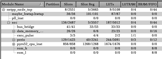
Risc-V 32 bit for netpp node
Yes, the RiscV fits on the netpp node with the existing ‘dagobert’ configuration:
- IRAM size: 0x8000
- DRAM size: 0x4000
- DMA scratch pad like with the ZPUng configuration: 2x 0x800
- 54 MHz core clock
Although the DRAM memory is DMA capable by principle, the scratch pad must be used for all fast I/O (networking) like on the ZPUng architecture. The reason for this are a few configurations reserved for the future, like shared memory between cache, pyrv32 and the DSP extension which use the dual ports of the block ram to read 64 bit instructions from certain memory portions.
The DMA default width however is 16 bit, unlike 8 bit as on the ZPUng. This allows for higher throughput, like 1G ethernet. Not making sense on the netpp node, but on a camera, for example.
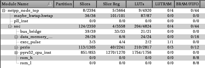
The tedious path to optimization
A lot of tweaking is necessary to crank f_max up to the possible maximum. Some tools will help you with that and point out stupid mistakes, with most of the synthesis tools it is a bit of trial and error and careful reading of the logfiles. These details are boring, so I will spare them here. Short version: You can get some interesting insight using the various floorplanning tools which can visualize signal and data paths between critical logic.
However, one may not want to go for maximum f_max, as most cycles are burnt elsewhere. Many things can be optimized in software or using clever DMA processing. This is where the CPU architecture is less relevant than a tricky SoC memory cross bar which allows the peripherals to use DMA while the CPU can do other things.
Optimization attack targets
There are a few deviations from the RISC-V standard you can look at:
- Implementing the CSR as memory mapped unit by replacing csr register exchange/set/clr commands through memory mapped I/O range accesses: This spares you some logic in the CPU and avoids further congestion close to the ALU
- Eliminating IRQ support all together by using DMA queues. This might appear odd, but for some data processing, pure DMA will do, and the main loop ends up to run deterministically.
CSR quirks
When implementing the CSR unit as memory mapped (to MMR space, i.e. memory mapped registers), there are a few quirks. First, remember that the CSRRS/CSRRC/CSRRW are supposed to be atomic, i.e. no emulation of the sort (1) Get register (2) or with value (3) write back is ok. Therefore this MMR mapped CSR needs to implement a W1C (write one to clear) respective W1S (…to set) logic. Because we only have write_enable or read_enable signals to the MMR I/O, W1C and W1S is to be implemented as shadow registers using an offset address.
Meaning, the register logic works as follows: An access to the CSR register 0xb05 will work with the following assembler instructions mapping, for example:
- CSRRW: A simultaneous read/write from/to address 0xffe0000 + (0x0b05 << 2)
- CSRRC: A W1C to 0xffe01000 + (0x0b05 << 2)
- CSRRS: A W1S to 0xffe02000 + (0x0b05 << 2)
Thus, the W1* logic is implemented in the peripherals for each register. Note: Since the CSR is sitting in MMR, a read is subject to a delay. Under certain circumstances, the pipeline may stall for one cycle, depending on the previous memory access history. This has to do with the 4/5-Pipeline shortcut/delaying mechanisms.
Optimization updates:
- 02 Oct 2019: no IRQ, pure DMA (no CSR), register file moved to LUT RAM, debug logic mostly eliminated:
+----------------------------------------------------------------------------------------------------------------------------------------------------------------------------------------------------------------------------------------------------------------------------------+
| Module                             | Partition | Slices*       | Slice Reg     | LUTs          | LUTRAM        | BRAM/FIFO | DSP48A1 | BUFG  | BUFIO | BUFR  | DCM   | PLL_ADV   | Full Hierarchical Name                                                                        |
+----------------------------------------------------------------------------------------------------------------------------------------------------------------------------------------------------------------------------------------------------------------------------------+
| ++pyrv32_cpu_inst                  |           | 347/348       | 354/354       | 1035/1036     | 44/44         | 0/0       | 0/0     | 0/0   | 0/0   | 0/0   | 0/0   | 0/0       | netpp_node_top/soc/pyrv32_cpu_inst                                                            |
Interesting. How does that compare to your ZPU in terms of speed (DMIPS)? Any plans on releasing this design?
I haven’t done any DMIPS comparison, but there are plans to integrate more benchmarks and tests into a test suite. Typically, the pyrv32 runs four times faster in my main loop — when comparing to the stripped down ZPUng (this has to do with many jumps to emulation microcode area).
Release as VHDL is planned, once I’ve got some more tests passed.