Posted on 8 Comments

netpp node evaluation platform

netpp node [Spartan6-LX9]

I am glad to announce a new user evaluation platform module called ‘netpp node’. Its motto is ‘IoT on FPGA done right’. See detailed specs and preliminary order information here: [ refdesigns/netpp_node ].

Update [21.12.]:

The netpp node engineering samples v0.0 have just passed the long term burn-in. Running since approx. 11 weeks non-stop, the units are flooded with netpp requests from an embedded PC and have shown no failure in the hardware, except a reboot resulting from a power outage.

v0.1 series [18.1]:

Received the series! So finally we can ramp up with the delivery to beta developers…(thanks for being so patient).

Analog I/O

ADC10 low level control

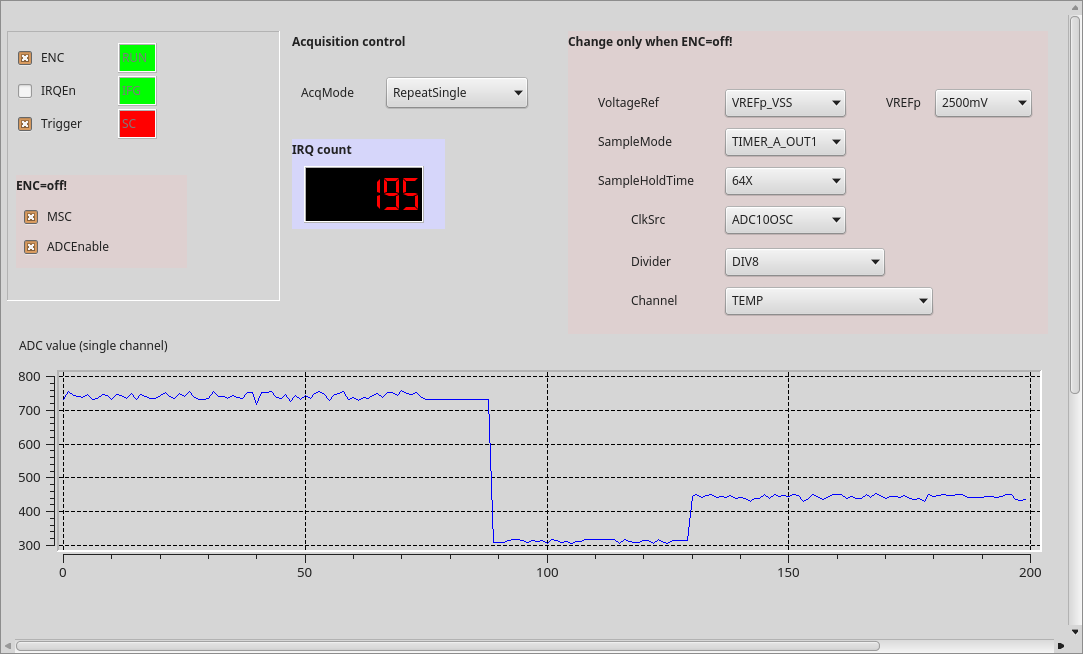
For analog I/O, U3 on the board is by default populated with a MSP430G2553, functioning as a smart ADC that is controlled from the ZPUng ‘dagobert’ SoC via i2c. All relevant ADC configuration registers are directly accessible via netpp. For instance, we access the low level registers through a process browser panel as shown above to play with the parameters. The process view panel automatically updates the volatile properties from the netpp peer device. The ADC10 variant of the netpp node provides up to six  analog channels internally sampled at up to 200ksps. When in synchronous acquisition configuration (SPI master), only five channels can be used.

Differential 16 bit sigma-delta ADC

SD16 analog input

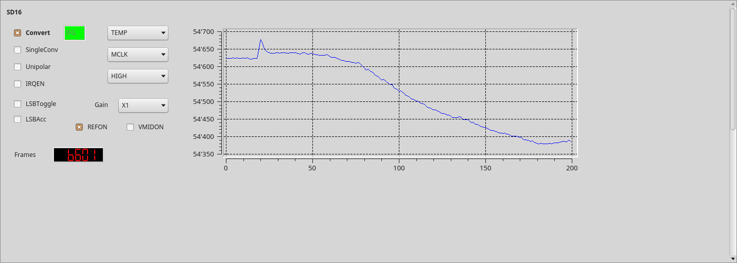
The alternate population option with a MSP430F2013 provides a Sigma-Delta 16 bit ADC with differential inputs and programmable gain amplifier. This variant provides three different input channel configurations using the provided analog input pins on this board. Moreover, the internal temperature is available in a separate channel.

‘Push on demand’ data streaming

By default, the analog sensors are polled, i.e. a measurement value is delivered upon request by the master. For synchronous sampling however, a ‘push’ strategy might be desired, where a netpp node delivers a value stream to a data logger or database. This can be netpp (where the netpp node acts as a master), however for high speed data transfers (‘network scope’), a low overhead UDP stream is more desirable. The dagobert SoC features a data port option with programmable slots to stream I/O channels as well as analog values using a standard real time protocol with 90 kHz time stamps.

Monitoring netpp packet performance

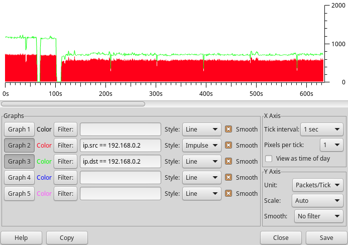
Packet behaviour in a real network is measured using the Wireshark protocol analyzer.

The figure below shows some example netpp transaction log that the netpp node handles at a very low CPU overhead based on direct register accesses.The red bars is the effective number of query responses using somewhat ineffective ping-pong requests. The performance can be increased by accumulating data into larger buffer properties.

For i2c or SPI transactions however, the packet rate is expected way lower.

For high speed performance like MJPEG video streaming, a separate UDP/RTP queue can be set up within the firmware to reach maximum throughput. However, there is no handshaking using this method.

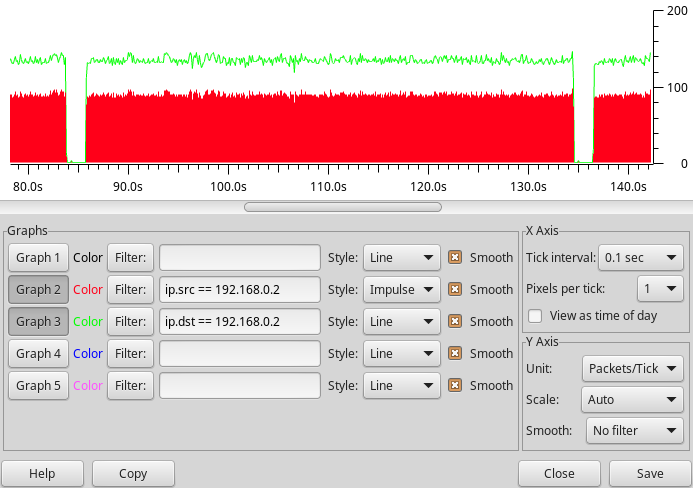
The image below shows a repeated property query from within Python. The pauses are introduced by external disturbance (stress test) that causes a packet drop – and the netpp engine to timeout and re-synchronize.

Python property query session

Improved RX/TX queue

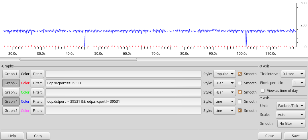
With an improved packet FIFO on FPGA, I was able to crank up the number of netpp requests per second, as shown in the Wireshark trace below. This test makes sure that several netpp clients can poll the netpp node at high frequencies without disturbing each other. The blue trace is a repeated poll of the full property tree, the red bars are the timed queries from a process viewer daemon. With no other disturbance, we get the occasional drops (e.g. at 45s, 101.5s) due to the queue running full


In-Field/System update

The default boot loader firmware supports self-programming over the cable. That means, the netpp_node can be supplied remotely with a new firmware image via a simple upgrade procedure over netpp. If the uploaded image is faulty, the system will fall back to the default boot loader. However, if the new design itself has errors, the system will be unable to recover  unless the reset button is pressed.

Test procedures

As the full model of this design is available for simulation, we can verify the system effectively against stress situations. In particular, network safety is of outmost importance. The test procedure check list of the dagobert SoC:

Completed

  • ARP and ping flooding
  • netpp packet performance test
  • Broken packet handling
  • Lost interrupt scenario (packet queue desynchronization)

Yet open

  • Jumbo packet flooding was tested, however support can not be enabled on this platform for the receiver queue. It is however possible under certain circumstances to generate (TX) Jumbo packets for experimental purposes. The performance gain is however minimal.

Extended RTOS support

Currently, the netpp node runs a simply bare metal main loop without particular RTOS functionality, i.e. all user code must be designed such that there are no blocking wait statements. Let me just put the FAQ together:

  • There is FreeRTOS and eCos support code for the ZPU architecture. However, I have no plans in going down that road, you’d be on your own.
  • A NuttX port is currently under evaluation and may likely be released in a few months time. NO PROMISES!
  • A simple ‘netpp OS’ with very basic task management is in experimental stage:
    • Guaranteed latency time from driver interrupt to queue handler task
    • ‘User space’ context switch when sleep() called
    • Very cheap context switches due to ZPU architecture improvements

Code size is an issue on this particular platform, larger programs (TCP stacks) need to move to the SPI flash overlay program space. Since this involves caching, the program timing is no longer fully deterministic and the RTOS functionality can only apply to program code running in the L1 memory.


Posted on

JPEG encoding on FPGA [revisited]

Although considered ‘ancient’ because invented in the early nineties, the JPEG standard is far from being dead or superseded. Its basic methods are still up to date for modern video compression.

For low latency image streaming, we have developed our own system on chip encoder solution ‘dorothea’ in 2013. It is based on the second generation L2 (a tag referring to ‘two lane’) JPEG engine, allowing JPEG compression of YCbCr 4:2:2 video at full pixelclock.

The ‘dorothea’ SoC is now superseded by the new ZPUng architecture, allowing more microcode tricks than on the previous MIPS based SoC. It is available as reference design ‘dombert’ (see SoC design overview) for UDP streaming up to 100 Mbps, optionally, 1G cores (third party) can be deployed as well for more throughput.

L2 example videos

These example videos are taken by direct capture (as coming from the camera) of the UDP video stream. The direct Bayer to YUV422 method is implemented in a microcode engine (license and patent free) and may still show visible artefacts, also, color correction is not implemented for this demo. For the live videos, a MT9M024 sensor on the HDR60 development kit has been used. Bit files for evaluation are available in the Reference Design section.

Posted on 2 Comments

ECP5G Versa board under Linux

The ECP5 platform has caught quite some attention a while ago, being on the rather high end with respect to GigaBit LVDS communication of all sorts. It’s the successor of the ECP3 which has been performing well with HDMI applications in the past.

Lattice Semiconductor had launched a Promo action for this Versa ECP5G board. With great assistance from Future Electronics Switzerland I was able to get hold of a devkit.

Running the Lattice Diamond toolchain on a Linux environment has so far been straightforward, with minor quirks on the GUI side. Let me revisit the important items to get up and running. If you happen to have a Linux OS installed that does not match the Lattice Semi recommendations for a development system, you might want to look at the Docker approach on how to set up the environment.

Programmer preparation

Porting a very simple CPU with UART interface to the platform, the final step is flashing things down into the board using the Lattice Diamond Programmer. Usually, when not having installed any udev rules, these are the steps you have to go through with root powers, in order to get the USB FTDI programmer interface recognized:

Bus 001 Device 013: ID 0403:6010 Future Technology Devices International, Ltd FT2232C Dual USB-UART/FIFO IC

According to this device enumeration, you give access to the device:

chmod a+rw /dev/bus/usb/001/013

and unbind the first ttyUSB0 device from the ftdi_sio driver – unfortunately, the Lattice driver is not able to unbind from within.

echo -n $TTY_ID > /sys/bus/usb/drivers/ftdi_sio/unbind

Replace $TTY_ID by the tty device entry in /sys/bus/usb/drivers/ftdi_sio/ that typically is of the form “1-3.2:1.0” (the trailing 0 stands for port A where the JTAG is at). If you have plugged in more than one FTDI adapter with UART capabilities, you will see several and need to figure out which is which.

Now you can download code into the programmer.

To automatize the process, you could also use the script below:

#/bin/bash

allow_io=`lsusb | sed -n 's/^Bus \([0-9]*\) Device \([0-9]*\): ID 0403:6010 .*/\1\/\2/p'`

unbind_tty=`ls /sys/bus/usb/drivers/ftdi_sio/ | sed -n 's/\(.*\:1\.0\).*/\1/p'`

sudo chmod a+rw \/dev\/bus\/usb\/$allow_io
sudo sh -c "echo $unbind_tty > /sys/bus/usb/drivers/ftdi_sio/unbind"

SPI flash download

When downloading your design into the SPI flash, make sure you have MASTER_SPI_PORT=ENABLED set in your *.lpf file. Otherwise the programmer will fail with an error report on CHECK_ID:

ERROR - Verification Error...when Processing function: 'CHECK_ID'

Then you’ll have to use the fast download (into SRAM) with an enabled Master SPI in order to be able to flash again.

Design issues

When starting to port our SoC design to this board, quite a few issues came up:

  • Don’t bother developing with Diamond v3.7. Some very obscure behaviour with wrong I/O mapping cost quite some headache. Seems to be solved in v3.8
  • v3.8 however is somewhat misleading with respect to output and return states from the Synopsys Synthesis engine ‘Synplify’. Make sure to check your design thoroughly, if Synplify throws an error, Diamond sometimes would not recognize that and map/PAR an old design netlist.
  • Weird random behaviour can occur under Linux with Diamond during PAR, like error messages with respect to path names. This seems to happen especially with long names and underscores. The behaviour has been around in many previous versions of Diamond, Tech Support has refused to accept this as a bug so far. The workaround is to call PAR using the command line (TCL) or use the Run Manager.
    Addendum: It seems that this bug is fixed in v3.9, but there is no release note about it.


Talking through the UART

In theory, you should be able to talk to your design through the UART (if your design supports it) by firing up minicom:

minicom -o -D /dev/ttyUSB1

Now here comes the catch: The default EEPROM from my Versa 5G board did not have a correct descriptor, however it came with the default VID:PID from FTDI, so the ftdi_sio driver would recognize it, but in fact not communicate, neither report an error.

So, in order to properly use this board, you may have to erase the EEPROM of the FTDI adapter on the Versa kit using FTDIs Mprog tool or alike. You might want to save the previous EEPROM content for reference, however it does not seem needed, the Programmer recognizes the Board just fine.

Finally, after downloading our SoC setup into the board, it is talking:

Booting, HW rev: 04 -- Running at 50 MHZ

------------- test shell -------------
-- ZpuSoC for Versa ECP5 --
-- (c) 2017 www.section5.ch --
-- type 'h' for help --
# 

Simulation issues

When trying to fully simulate the SoC setup with PLL primitives and some instanced ip cores created by the Clarity module (obviously that’s the IPExpress descendant for ECP5), it turns out that some of the simulation primitives for the VHDL side are missing.

Some of them could be converted using the VHDL conversion trick from Icarus Verilog by the following Makefile rule:

%.vhdl: %.v
    iverilog -tvhdl -o $@ -pdepth=1 $<

However, some of the needed components might not convert without additional tweaking. Hopefully, Lattice Semi will come out with updated VHDL libraries.

IPcore simulation under GHDL

When generating IP cores that depend on library items and running them through GHDL, you might see this error message:

warning: component instance "scuba_vlo_inst" is not bound

However, if you have prepared your FPGA primitive components library, like ecp5um-obj93.cf right, the primitive simulation models should be in there (search for ‘vlo’ in the *.cf file if in doubt).

The reason why this is happening is that there could be component prototype declarations in the IP core file that shouldn’t be there in order to reference to the components from the library. So: Just remove the “component” declaration sections and all should link fine. The drawback of this is, that you need two IP core versions, one for simulation and one for synthesis. If you have a better solution, let me know.

Next steps

Now, the fancy stuff on this board to be evaluated is:

  • DDR3 memory
  • Two GigE capable interfaces

Also, the ECP5 on this board has enough resources to run several ZPUng cores simultaneously. For safety reasons, we wouldn’t want the IoT crap run in the same environment as our controlling main loop.

Therefore, a second processor (Core B) is instanced for running the Ethernet Stack (lwip) only, while maintaining a simple DMA channel to the controller Core A for communication. If core B is compromised, Core A will still maintain its “hardened” control loop and not go haywire.

Implementing DDR3 is tricky. Therefore you might want to use the DDR3 IP core supplied by Lattice. On the demo kit, it will work for a few hours and then pull the global reset.

Networking

Of course, I was very curious about the Ethernet ports on this board. It’s armed with two GigE capable Marvell Phys whose data sheets are a little hard to get hold of, but one might also look at various source code around the web or just check the reference design from Lattice. The reference design uses lwip, since I only need and want UDP, I ported a zerocopy-capable UDP stack I developed for the Blackfin EMAC to the ZPUng SoC (“cranach”), which is equipped with some DMA capable scratch pad memory for a proper packet queue.

After all, the FPGA is now able to speak netpp, so I can turn on an LED for example:

> netpp UDP:192.168.05:2016 LED.Yellow 1

Resource usage

You might want to know how much logic and RAM is consumed by this solution.

Design Summary
   Number of registers:   2770 out of 44457 (6%)
      PFU registers:         2767 out of 43848 (6%)
      PIO registers:            3 out of   609 (0%)
   Number of SLICEs:      2963 out of 21924 (14%)
      SLICEs as Logic/ROM:   2891 out of 21924 (13%)
      SLICEs as RAM:           72 out of 16443 (0%)
      SLICEs as Carry:        309 out of 21924 (1%)
   Number of LUT4s:        4154 out of 43848 (9%)
   Number of block RAMs:  28 out of 108 (26%)
   Number of DCS:  1 out of 2 (50%)
   Number of PLLs:  1 out of 4 (25%)

As for the actual program code, containing:

  • UDP stack supporting ARP, ICMP ping
  • Minimal shell (UART)
  • System I/O drivers (UART, Timer, MAC, PWM)
  • netpp minimal server with some LED handling

This is what’s effectively downloaded into the target:

(gdb) init
Loading section .fixed_vectors, size 0x400 lma 0x0
Loading section .l1.text, size 0x4af5 lma 0x400
Loading section .rodata, size 0x168 lma 0x4ef8
Loading section .rodata.str1.4, size 0xf60 lma 0x5060
Loading section .data, size 0x2c0 lma 0x5fc0
Start address 0x0, load size 25213


There’s a significant amount of string data for debugging in the .rodata.str1.4 section due to debugging info, plus some netpp descriptors. These again could be ‘overlayed’ to the SPI flash, as they are not too frequently accessed. To be investigated next…